
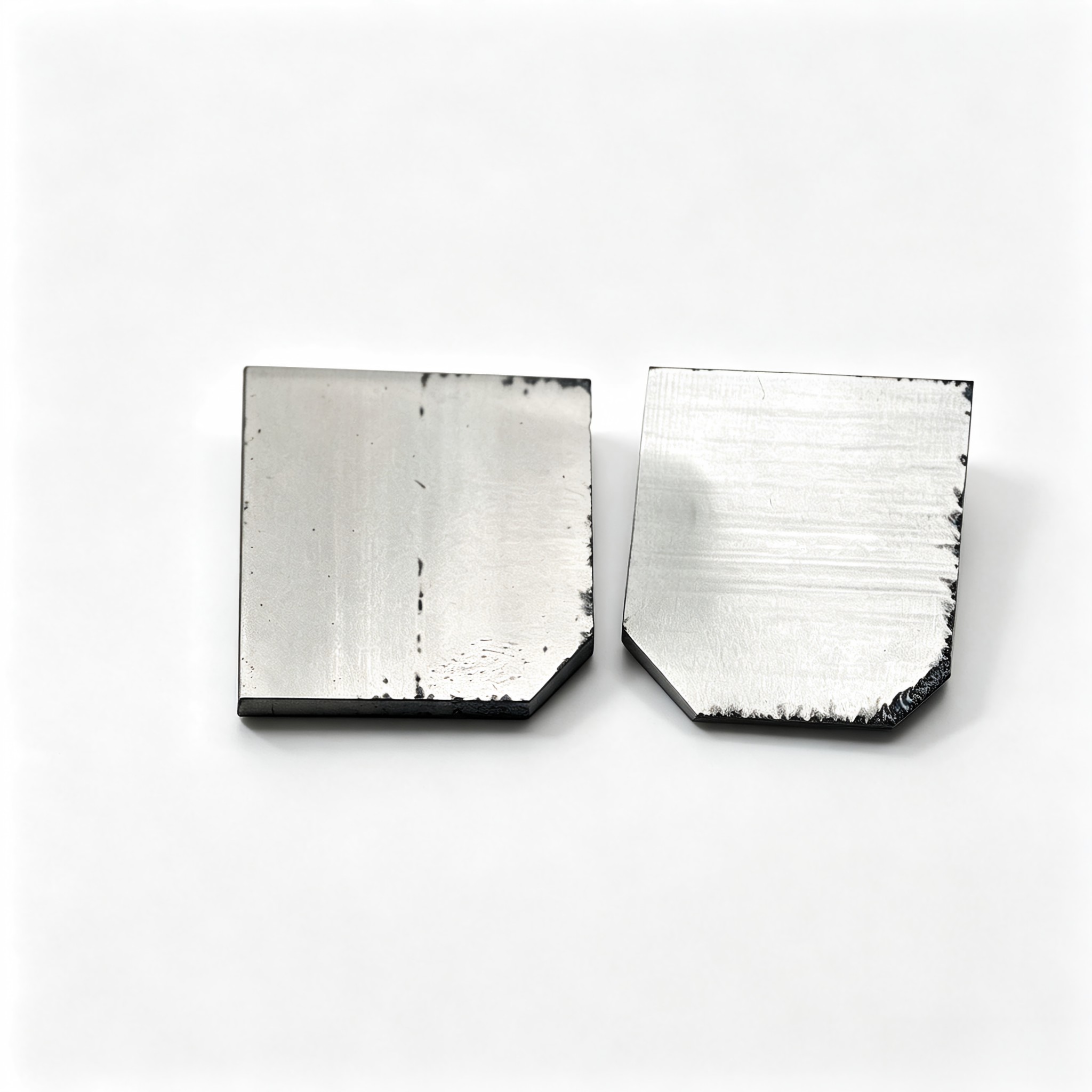
Single-Crystal Diamond
MPCVD-grown single-crystal diamond in standard plate sizes from 7×7 mm to 25×25 mm, for high-performance electronics and functional materials. A material platform for heat spreading in high-heat-flux devices and for advanced device R&D and validation.
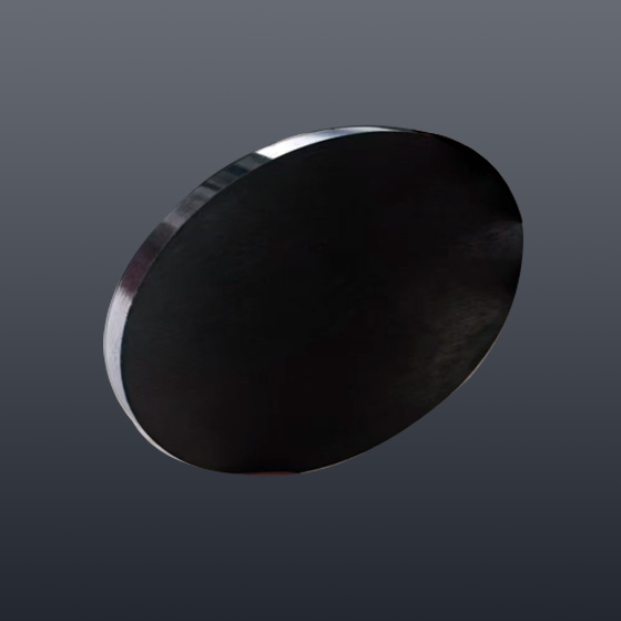
Polycrystalline Diamond Heat Spreader
For high-heat-flux electronic devices, with high thermal conductivity, low thermal expansion, and electrically insulating heat spreading. A candidate material for next-generation high-performance heat spreading.
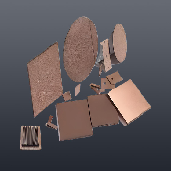
Copper-Metallized Single-Crystal Diamond
A thermally conductive, electrically insulating material with a single-crystal diamond core and a copper layer bonded to the surface, combining ultra-high thermal conductivity with electrical isolation.
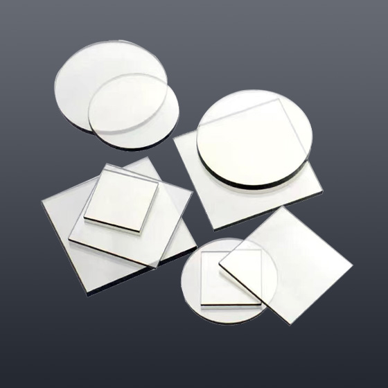
Diamond Optical Window
An MPCVD-grown diamond optical window, with broad spectral transmission, high thermal conductivity, and strong chemical stability, for high-power lasers, infrared detection, and optical systems in extreme environments.

8-Inch Heteroepitaxial Diamond Wafer Platform
Research-stage 8-inch diamond wafers grown by MPCVD heteroepitaxy on gallium nitride, sapphire, and silicon carbide, as a material platform for next-generation power electronics, RF devices, and semiconductor thermal management.
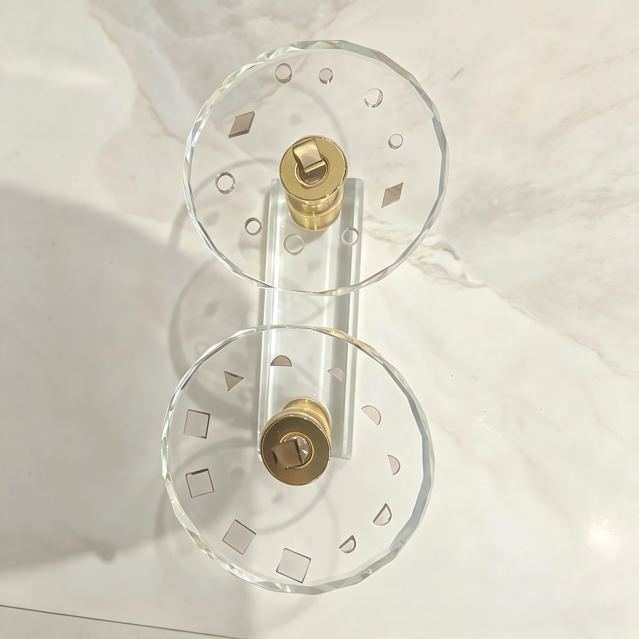
Diamond Tool Blank
A high-performance tool blank precision-cut from single-crystal diamond plate. It supplies the cutting edge for turning tools, milling tools, drills, and grinding tools made by downstream precision-machining companies.
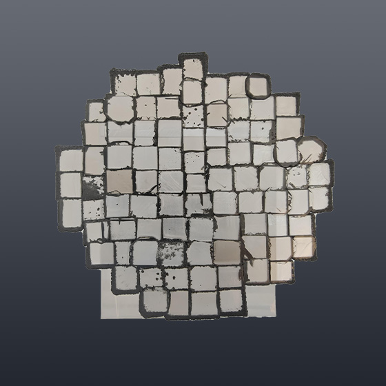
Single-Crystal Diamond Rough
Raw blocks separated from MPCVD-grown single-crystal diamond after an initial cut. The starting material for later substrate processing, optical windows, and electronic-grade functional materials.

Aluminum-Metallized Single-Crystal Diamond
A thermally conductive, electrically insulating material with a single-crystal diamond core and an aluminum layer bonded to the surface, combining ultra-high thermal conductivity, electrical isolation, and light weight.
Specifications and customization
Beyond standard sizes, the dimensions below can be adjusted to the application. The workable range follows the technical assessment.
Size
Planar size follows the device layout and assembly space.
Thickness
The thickness range follows the thermal-resistance budget and the mechanical-strength requirement.
Surface condition
As-grown, lapped, or polished, chosen for the next process.
Processing method
Laser cutting, chamfering, drilling, and metallization, combined as needed.
Tell us your application scenario
Share the power density, size limits, or process window, and we will help confirm a suitable material form and processing route.