
Ultra-high thermal conductivity: system-equivalent thermal conductivity of 1200–2000 W/(m·K), significantly higher than conventional Cu-Mo (CMC), Cu-W (CPC), and other metal-matrix heat-spreading materials (typically in the 150–300 W/(m·K) range).
DIAMOND-ON-COPPER (CU-METALLIZED SINGLE CRYSTAL DIAMOND)
Copper-Metallized Single-Crystal Diamond
Diamond-on-Copper (Cu-Metallized Single Crystal Diamond)
High-thermal-conductivity, electrically insulating material with single-crystal diamond as the heat-conducting core and a bonded copper surface layer—combining ultra-high thermal conductivity with electrical isolation.
QS / PRODUCT PLATFORM
MPCVD
01 / PRODUCT OVERVIEW
Product overview
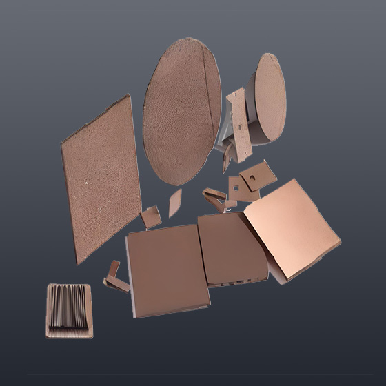
Copper-metallized single-crystal diamond uses single-crystal diamond as the primary heat conductor. Through surface metallization bonding, a copper metal layer is joined to the diamond surface, forming a "core + cladding" layered structure.
This structure differs fundamentally from "diamond–copper composite" (an isotropic bulk material in which diamond micropowder particles are dispersed throughout a copper matrix): the latter is electrically conductive throughout; copper-metallized single-crystal diamond uses the single-crystal diamond body as an insulating core, with a conductive metal interface only on the surface—two distinct structural and performance routes.
This structure combines diamond’s intrinsic ultra-high thermal conductivity and electrical insulation with a copper layer that is solderable, machinable, and suitable for electrical interconnect—an ideal heat-spreading material for next-generation high-heat-flux devices.
01
MPCVD growth
02 / MATERIAL CHARACTERISTICS
Key advantages
Copper-Metallized Single-Crystal Diamond
High thermal diffusivity: thermal diffusivity 9.0–9.5 cm²/s for fast thermal response under high-heat-flux transient conditions.
Integrated thermal conduction and electrical isolation: the diamond core is intrinsically insulating (volume resistivity 2.95×10¹³ Ω·cm); the copper layer is conductive and solderable—delivering "high thermal conductivity + electrical isolation" in one stack, unlike bulk-conductive diamond–copper composites.
Low and stable CTE: thermal expansion coefficient 3.1962×10⁻⁶/K over RT–700°C, with low thermal-mismatch risk versus semiconductor devices.
Structure and dimensions customizable: thickness 300–5000 μm on request; metallization (copper / Au plating / optional tin) and patterned vias customizable to customer needs.
03 / TECHNICAL HIGHLIGHTS
Technical parameters
Crystal parameters
Square or rectangular substrate (same as the single-crystal diamond line)
—
Form
7×7, 8×8, 10×12, 11×13, 13×15, 15×15, 25×25
mm
Standard sizes
300–5,000 (that is 0.3–5 mm); special requirements can be customized
μm
Thickness
3.51–3.52
g/cm³
Bulk density
| Item | Unit | Specification |
|---|---|---|
| Form | — | Square or rectangular substrate (same as the single-crystal diamond line) |
| Standard sizes | mm | 7×7, 8×8, 10×12, 11×13, 13×15, 15×15, 25×25 |
| Thickness | μm | 300–5,000 (that is 0.3–5 mm); special requirements can be customized |
| Bulk density | g/cm³ | 3.51–3.52 |
Thermal performance
| Item | Unit | Specification |
|---|---|---|
| Thermal conductivity (system equivalent) | W/(m·K) | 1200–2000 |
| Thermal diffusivity | cm²/s | 9.0–9.5 |
| Thermal expansion coefficient (RT–700°C) | 10⁻⁶/K | 3.1962 |
Mechanical performance
| Item | Unit | Specification |
|---|---|---|
| Mohs hardness | — | ≥10 |
| Tensile strength | MPa | 450–1100 |
| Young's modulus | GPa | 1000–1100 |
Electrical performance
| Item | Unit | Specification |
|---|---|---|
| Dielectric constant (1 MHz) | — | 5.68 |
| Dielectric loss (1 MHz) | — | 6.2×10⁻⁸ |
| Volume resistivity (25°C) | Ω·cm | 2.95×10¹³ |
| Dielectric strength | V/mA | DC 5.5KV/1.5mA |
Metallization & solder & via drilling
| Item | Specification |
|---|---|
| Metallization | Gold plating or copper cladding; optional tin surface finish so the customer can solder with paste reflow |
| Solder | AuSn and similar |
| Drilling | Metallization and patterning can be customized |
04 / SPECIFICATIONS
Product specifications
Standard sizes
7×7 mm
8×8 mm
10×12 mm
11×13 mm
13×15 mm
15×15 mm
25×25 mm
THICKNESS
0.3–5 mm (300–5000 μm); special requirements customizable
Standard sizes: square/rectangular substrates 7×7 mm, 8×8 mm, 10×12 mm, 11×13 mm, 13×15 mm, 15×15 mm, 25×25 mm (aligned with the standard sizes on the "single-crystal diamond" product page)
Thickness range: 0.3–5 mm (300–5000 μm); special requirements customizable
Customizable: substrate morphology, size, thickness, metallization scheme
Metallization and surface options: Au plating / copper metallization as standard; optional tin plating for direct solder-paste reflow; solder compatibility including AuSn; patterning/via drilling customizable on request
06 / APPLICATIONS
Application fields

Lasers

Microwave power devices

High-power semiconductor lighting

Cooling for high-power IC chip packages
Insulating heat-spreader substrates for power modules (IGBT, SiC, GaN power devices, EV traction inverters, and other use cases needing both high thermal conductivity and electrical isolation)
07 / QUALITY & VALIDATION
Inspection and documentation
No publicly available product-specific third-party inspection report for copper-metallized single-crystal diamond has been confirmed yet.